Intel Kicks Off Fab Co-Investment Program with Brookfield: New Fabs to be Jointly Owned

Intel this week introduced its new Semiconductor Co-Investment Program (SCIP) under which it will build new manufacturing facilities in collaboration with investment partners – a sharp departure from the company’s traditional stance of wholly owning its logic fabs. As part of its SCIP initiative, Intel has already signed a deal with Brookfield Asset Management, which will provide Intel about $15 billion to build its fab new fab in Arizona in exchange for a 49% stake in the project. Furthermore, similar co-investment models are set to be used for other fabs in the future.
New Fabs Are Getting Costlier
When Intel announced plans to produce chips for other companies last year (and to a large degree become a contract maker of semiconductors), it marked a significant shift in the company’s business strategy that required Intel to build new manufacturing capacity not only for itself, but for its future clients as well. But modern fabs are exceptionally expensive, as new manufacturing tools — such as contemporary extreme ultraviolet (EUV) lithography scanners — are prohibitively expensive, which makes it considerably harder for the company to execute on its IDM 2.0 strategy from capital point of view.
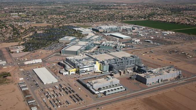
To get sufficient capacity for its own products and for its fabless clients in the mid-term future, Intel had to engage into several capital-intensive projects: the $7.1 billion fab expansion in Ireland (which has probably been completed); two new fabs — Fab 52 and Fab 62 — at its Ocotillo site near Chandler, Arizona that were expected to cost $20 billion; an all-new semiconductor production campus in Ohio that will need $20 billion initially and will be a size of a small town as well as will cost up to $100 when fully built; and an all-new production facility near Magdeburg, Germany (which will require an investment of €17 billion).
Intel is set to get billions in incentives from local authorities as well as subsidies from federal governments of the U.S. and Germany to build these fabs. But modern EUV-capable semiconductor production facilities cost about $10 billion (large gigafabs with a capacity of 100,000 wafer starts per month cost north from $20 billion), so financing these projects is particularly challenging even for Intel. Therefore, in a bid to build its new facilities in Arizona the company decided to engage into its co-investment program with Brookfield.
Intel to Maintain Majority Ownership
Under the terms of the deal, the two companies will co-invest $30 billion in the ongoing expansion of the site with Intel financing 51% and Brookfield backing 49% of the total project cost. Previously Intel planned to invest $20 billion in its Fab 52 and Fab 62, but together with Brookfield the sum has increased to $30 billion. In addition to getting access to additional funding, Intel could also take advantage of Brookfield’s experience in developing infrastructure assets.
By working together with Brookfield, Intel will get $15 billion in free cash flow and will be able to invest more into its new fabs without raising new debt. Also, this will allow Intel to invest more in other projects while “continuing to fund a healthy and growing dividend.” Meanwhile, the $15 billion benefit is “expected to be accretive to Intel’s earnings per share during the construction and ramp phase.”
Perhaps the key part of the announcement is the fact that Intel plans to sign similar deals with co-investors in the future, so expect its upcoming manufacturing capacity to be co-funded by others. Intel will retain majority ownership and operating control of its chip factories, but it will not own 100% of them. Previously the company rarely engaged into joint ventures, the most notable exceptions being IMFT, the company’s NAND flash joint-venture with Micron, and participating in ASML’s customer co-investment program from early 2010s.
“This landmark arrangement is an important step forward for Intel’s Smart Capital approach and builds on the momentum from the recent passage of the CHIPS Act in the U.S.,” said David Zinsner, Intel CFO. “Semiconductor manufacturing is among the most capital-intensive industries in the world, and Intel’s bold IDM 2.0 strategy demands a unique funding approach. Our agreement with Brookfield is a first for our industry, and we expect it will allow us to increase flexibility while maintaining capacity on our balance sheet to create a more distributed and resilient supply chain.”
Co-ownership of semiconductor manufacturing facilities is not something unheard of the industry. China’s Semiconductor Manufacturing International Co. (SMIC) invests in new fabs together with local authorities of Chinese provinces as well as various asset management companies and/or investment banks (many of which are controlled by China’s federal government). GlobalFoundries used to be co-owned by AMD and Mubadala before the latter acquired AMD’s stake as the chip developer badly needed money. Yet, a co-investment program is something particularly new for Intel, which has always owned 100% of its manufacturing facilities. Ultimately, as it looks like as the semiconductor production is getting more expensive, there is a first time for anything.