Micro Advantage

AMD Announces Ryzen 7000 Reveal Livestream for August 29th

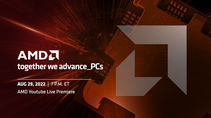
In a brief press release sent out this morning, AMD has announced that they will be delivering their eagerly anticipated Ryzen 7000 unveiling later this month as a live stream. In an event dubbed “together we advance_PCs”, AMD will be discussing the forthcoming Ryzen 7000 series processors as well as the underlying Zen 4 architecture and associated AM5 platform – laying the groundwork ahead of AMD’s planned fall launch for the Ryzen 7000 platform. The event is set to kick off on August 29th at 7pm ET (23:00 UTC), with CEO Dr. Lisa Su and CTO Mark Papermaster slated to present.

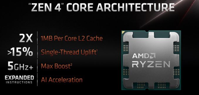
AMD first unveiled their Ryzen 7000 platform and branding back at Computex 2022, offering quite a few high-level details on the forthcoming consumer processor platform while stating it would be launching in the fall. The new CPU family will feature up to 16 Zen 4 cores using TSMC’s optimized 5 nm manufacturing process for the Core Complex Die (CCD), and TSMC’s 6nm process for the I/O Die (IOD). AMD has not disclosed a great deal about the Zen 4 architecture itself, though their Computex presentation has indicated we should expect a several percent increase in IPC, along with a further several percent increase in peak clockspeeds, allowing for a 15%+ increase in single-threaded performance.

The Ryzen 7000 series is also notable for being the first of AMD’s chiplet-based CPUs to integrate a GPU – in this case embedding it in the IOD. The modest GPU allows for AMD’s CPUs to supply their own graphics, eliminating the need for a discrete GPU just to boot a system while, we expect, providing enough performance for basic desktop work.

AMD Desktop CPU Generations
AnandTech Ryzen 7000
(Raphael)
Ryzen 5000
(Vermeer)
Ryzen 3000
(Matisse)
CPU Architecture Zen 4 Zen 3 Zen 2
CPU Cores Up To 16C / 32T Up To 16C / 32T Up To 16C / 32T
GPU Architecture RDNA2 N/A N/A
GPU Cores TBD N/A N/A
Memory DDR5 DDR4 DDR4
Platform AM5 AM4 AM4
CPU PCIe Lanes 24x PCIe 5.0 24x PCIe 4.0 24x PCIe 4.0
Manufacturing Process CCD: TSMC N5
IOD: TSMC N6
CCD: TSMC N7
IOD: GloFo 12nm
CCD: TSMC N7
IOD: GloFo 12nm

The new CPU family will also come with a new socket and motherboard platform, which AMD is dubbing AM5. The first significant socket update for AMD in six years will bring with it a slew of changes and new features, including a switch to an LGA-style socket (LGA1718) and support for DDR5 memory. Providing the back-end for AM5 will be AMD’s 600 series chipsets, with AMD set to release both enthusiast and mainstream chipsets. PCIe 5.0 will also be supported by the platform, but in the interest of keeping motherboard prices in check, it is not a mandatory motherboard feature.

The remaining major disclosures that AMD hasn’t made – and which we’re expecting to see at their next event – will be around the Zen 4 architecture itself, as well as information on specific Ryzen 7000 SKUs. Pricing information is likely not in the cards (the industry has developed a strong tendency to announce prices at the last minute), but at the very least we should have an idea of how many cores to expect on the various SKUs, as well as where the official TDPs will land in this generation given AM5’s greater power limits.

Meanwhile, AMD’s press release does not mention whether the presentation will be recorded or live. Like most tech companies, AMD switched to pre-recorded presentations due to the outbreak of COVID-19, which in turn has been paying dividends in the form of breezier and more focused presentations with higher production values. While relatively insignificant in the big picture of things, it will be interesting to see whether AMD is going back to live presentations for consumer product unveils such as this.

In any case, we’ll find out more during AMD’s broadcast. The presentation is slated to air on August 29th at 7pm Eastern, on AMD’s YouTube channel. And of course, be sure to check out AnandTech for a full rundown and analysis of AMD’s announcements.

UCIe Consortium Incorporates, Adds NVIDIA and Alibaba As Members

Among the groups with a presence at this year’s Flash Memory Summit is the UCIe Consortium, the recently formed group responsible for the Universal Chiplet Interconnect Express (UCIe) standard. First unveiled back in March, the UCIe Consortium is looking to establish a universal standard for connecting chiplets in future chip designs, allowing chip builders to mix-and-match chiplets from different companies. At the time of the March announcement, the group was looking for additional members as it prepared to formally incorporate, and for FMS they’re offering a brief update on their progress.

First off, the group has now become officially incorporated. And while this is largely a matter of paperwork for the group, it’s none the less an important step as it properly establishes them as a formal consortium. Among other things, this has allowed the group to launch their work groups for developing future versions of the standard, as well as to offer initial intellectual property rights (IPR) protections for members.

More significant, however, is the makeup of the incorporated UCIe board. While UCIe was initially formed with 10 members – a veritable who’s who of many of the big players in the chip industry – there were a couple of notable absences. The incorporated board, in turn, has picked up two more members who have bowed to the peer (to peer) pressure: NVIDIA and Alibaba.

NVIDIA for its part has already previously announced that it would support UCIe in future products (even if it’s still pushing customers to use NVLink), so their addition to the board is not unexpected. Still, it brings on board what’s essentially the final major chip vendor, firmly establishing support for UCIe across all of the ecosystem’s big players. Meanwhile, like Meta and Google Cloud, Alibaba represents another hyperscaler joining the group, who will presumably be taking full advantage of UCIe in developing chips for their datacenters and cloud computing services.

Overall, according to the Consortium the group is now up to 60 members total. And they are still looking to add more through events like FMS as they roll on towards getting UCIe 1.0 implemented in production chiplets.

Compute Express Link (CXL) 3.0 Announced: Doubled Speeds and Flexible Fabrics

While it’s technically still the new kid on the block, the Compute Express Link (CXL) standard for host-to-device connectivity has quickly taken hold in the server market. Designed to offer a rich I/O feature set built on top of the existing PCI-Express standards – most notably cache-coherency between devices – CXL is being prepared for use in everything from better connecting CPUs to accelerators in servers, to being able to attach DRAM and non-volatile storage over what’s physically still a PCIe interface. It’s an ambitious and yet widely-backed roadmap that in three short years has made CXL the de facto advanced device interconnect standard, leading to rivals standards Gen-Z, CCIX, and as of yesterday, OpenCAPI, all dropping out of the race.

And while the CXL Consortium is taking a quick victory lap this week after winning the interconnect wars, there is much more work to be done by the consortium and its members. On the product front the first x86 CPUs with CXL are just barely shipping – largely depending on what you want to call the limbo state that Intel’s Sapphire Ridge chips are in – and on the functionality front, device vendors are asking for more bandwidth and more features than were in the original 1.x releases of CXL. Winning the interconnect wars makes CXL the king of interconnects, but in the process, it means that CXL needs to be able to address some of the more complex use cases that rival standards were being designed for.

To that end, at Flash Memory Summit 2022 this week, the CXL Consortium is at the show to announce the next full version of the CXL standard, CXL 3.0. Following up on the 2.0 standard, which was released at the tail-end of 2020 and introduced features such as memory pooling and CXL switches, CXL 3.0 focuses on major improvements in a couple of critical areas for the interconnect. The first of which is the physical side, where is CXL doubling its per-lane throughput to 64 GT/second. Meanwhile, on the logical side of matters, CXL 3.0 is greatly expanding the logical capabilities of the standard, allowing for complex connection topologies and fabrics, as well as more flexible memory sharing and memory access modes within a group of CXL devices.

OpenCAPI to Fold into CXL – CXL Set to Become Dominant CPU Interconnect Standard

With the 2022 Flash Memory Summit taking place this week, not only is there a slew of solid-state storage announcements in the pipe over the coming days, but the show is also increasingly a popular venue for discussing I/O and interconnect developments as well. Kicking things off on that front, this afternoon the OpenCAPI and CXL consortiums are issuing a joint announcement that the two groups will be joining forces, with the OpenCAPI standard and the consortium’s assets being transferred to the CXL consortium. With this integration, CXL is set to become the dominant CPU-to-device interconnect standard, as virtually all major manufacturers are now backing the standard, and competing standards have bowed out of the race and been absorbed by CXL.

Pre-dating CXL by a few years, OpenCAPI was one of the earlier standards for a cache-coherent CPU interconnect. The standard, backed by AMD, Xilinx, and IBM, among others, was an extension of IBM’s existing Coherent Accelerator Processor Interface (CAPI) technology, opening it up to the rest of the industry and placing its control under an industry consortium. In the last six years, OpenCAPI has seen a modest amount of use, most notably being implemented in IBM’s POWER9 processor family. Like similar CPU-to-device interconnect standards, OpenCAPI was essentially an application extension on top of existing high speed I/O standards, adding things like cache-coherency and faster (lower latency) access modes so that CPUs and accelerators could work together more closely despite their physical disaggregation.

But, as one of several competing standards tackling this problem, OpenCAPI never quite caught fire in the industry. Born from IBM, IBM was its biggest user at a time when IBM’s share in the server space has been on the decline. And even consortium members on the rise, such as AMD, ended up skipping on the technology, leveraging their own Infinity Fabric architecture for AMD server CPU/GPU connectivity, for example. This has left OpenCAPI without a strong champion – and without a sizable userbase to keep things moving forward.

Ultimately, the desire of the wider industry to consolidate behind a single interconnect standard – for the sake of both manufacturers and customers – has brought the interconnect wars to a head. And with Compute Express Link (CXL) quickly becoming the clear winner, the OpenCAPI consortium is becoming the latest interconnect standards body to bow out and become absorbed by CXL.

Under the terms of the proposed deal – pending approval by the necessary parties – the OpenCAPI consortium’s assets and standards will be transferred to the CXL consortium. This would include all of the relevant technology from OpenCAPI, as well as the group’s lesser-known Open Memory Interface (OMI) standard, which allowed for attaching DRAM to a system over OpenCAPI’s physical bus. In essence, the CXL consortium would be absorbing OpenCAPI; and while they won’t be continuing its development for obvious reasons, the transfer means that any useful technologies from OpenCAPI could be integrated into future versions of CXL, strengthening the overall ecosystem.

With the sublimation of OpenCAPI into CXL, this leaves the Intel-backed standard as dominant interconnect standard – and the de facto standard for the industry going forward. The competing Gen-Z standard was similarly absorbed into CXL earlier this year, and the CCIX standard has been left behind, with its major backers joining the CXL consortium in recent years. So even with the first CXL-enabled CPUs not shipping quite yet, at this point CXL has cleared the neighborhood, as it were, becoming the sole remaining server CPU interconnect standard for everything from accelerator I/O (CXL.io) to memory expansion over the PCIe bus.

<div>The Intel Core i9-12900KS Review: The Best of Intel’s Alder Lake, and the Hottest</div>

As far as top-tier CPU SKUs go, Intel’s Core i9-12900KS processor sits in noticeably sharp In contrast to the launch of AMD’s Ryzen 7 5800X3D processor with 96 MB of 3D V-Cache. Whereas AMD’s over-the-top chip was positioned as the world’s fastest gaming processor, for their fastest chip, Intel has kept their focus on trying to beat the competition across the board and across every workload.

As the final 12th Generation Core (Alder Lake) desktop offering from Intel, the Core i9-12900KS is unambiguously designed to be the powerful one. It’s a “special edition” processor, meaning that it’s low-volume, high-priced chip aimed at customers who need or want the fastest thing possible, damn the price or the power consumption.

It’s a strategy that Intel has employed a couple of times now – most notably with the Coffee Lake-generation i9-9900KS – and which has been relatively successful for Intel. And to be sure, the market for such a top-end chip is rather small, but the overall mindshare impact of having the fastest chip on the market is huge. So, with Intel looking to put some distance between itself and AMD’s successful Ryzen 5000 family of chips, Intel has put together what is meant to be the final (and fastest) word in Alder Lake CPU performance, shipping a chip with peak (turbo) clockspeeds ramped up to 5.5GHz for its all-important performance cores.

For today’s review we’re putting Alder Lake’s fastest to the test, both against Intel’s other chips and AMD’s flagships. Does this clockspeed-boosted 12900K stand out from the crowd? And are the tradeoffs involved in hitting 5.5GHz worth it for what Intel is positioning as the fastest processor in the world? Let’s find out.